Innovation Hub Semiconductor: Metrology and inspection are becoming increasingly important
Our first Innovation Hub in Semiconductor Metrology and Inspection (SeMI) was established at Park Innovaare to turn cutting-edge ideas into real-world impact. Located next to Switzerland’s largest research institute Paul Scherrer Institute PSI, partner companies enjoy simple access to its world-class research expertise, state-of-the-art cleanrooms, prototyping facilities, and large-scale infrastructure - all designed to fuel innovation and accelerate progress. As your gateway to world‑class R&D, SeMI serves as an on‑site collaborator, keeping our partners ahead of the curve and driving the next era of semiconductor innovation.
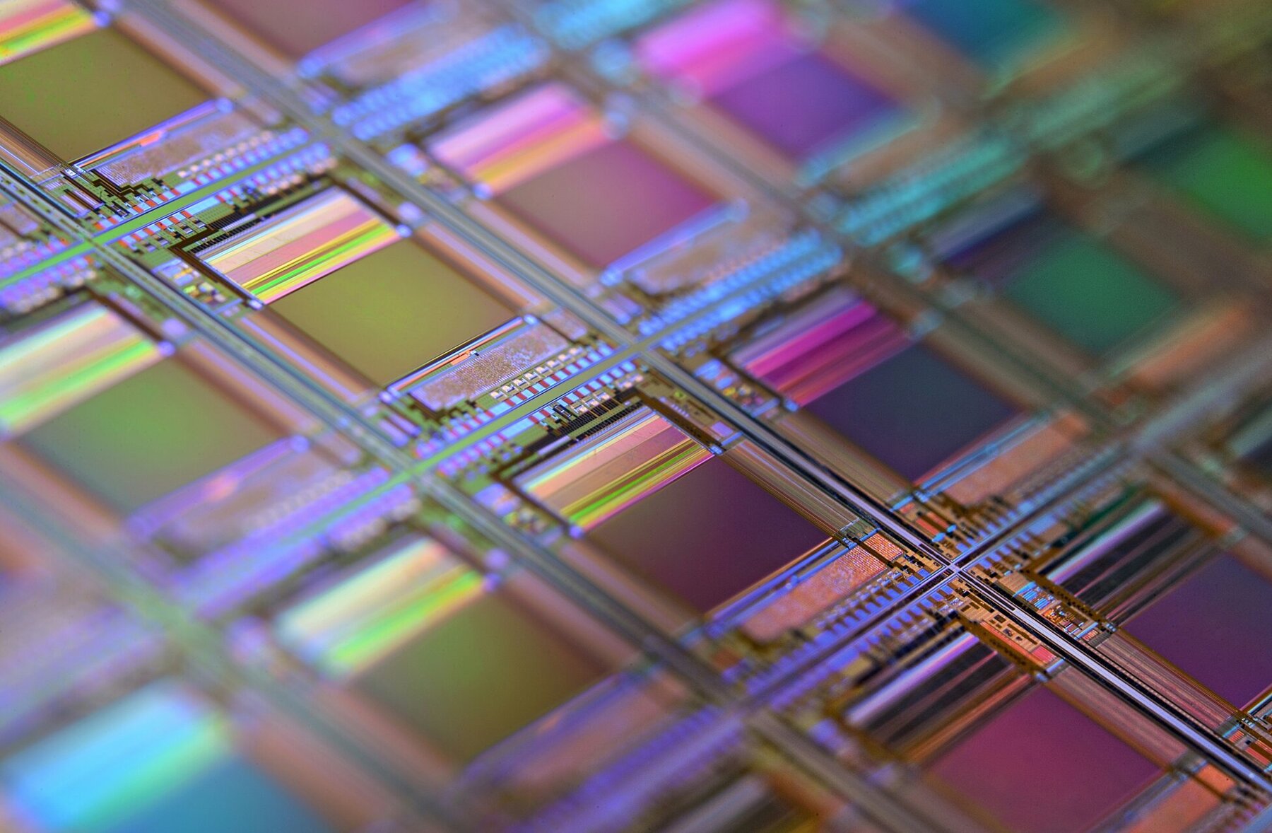
As the semiconductor industry enters the Angstrom era, the shift toward GAA (Gate-All-Around) and CFET (Complementary Field-Effect Transistor) architectures - alongside denser memory and heterogeneous integration - has made early defect detection a critical factor in driving manufacturing yield. With feature sizes shrinking well below the 10 nm threshold, traditional metrology is reaching a critical bottleneck. In this landscape, new solutions are required to ensure the viability of the next generation of AI and high-performance computing hardware.
Project Manager SeMI Innovation Hub,
Park Innovaare
“Precision measurement technology and testing form the backbone of profitable chip manufacturing. We have launched this hub to strengthen our partners’ long-term competitiveness through shared resources and strategic R&D collaborations.”
Events and Workshops
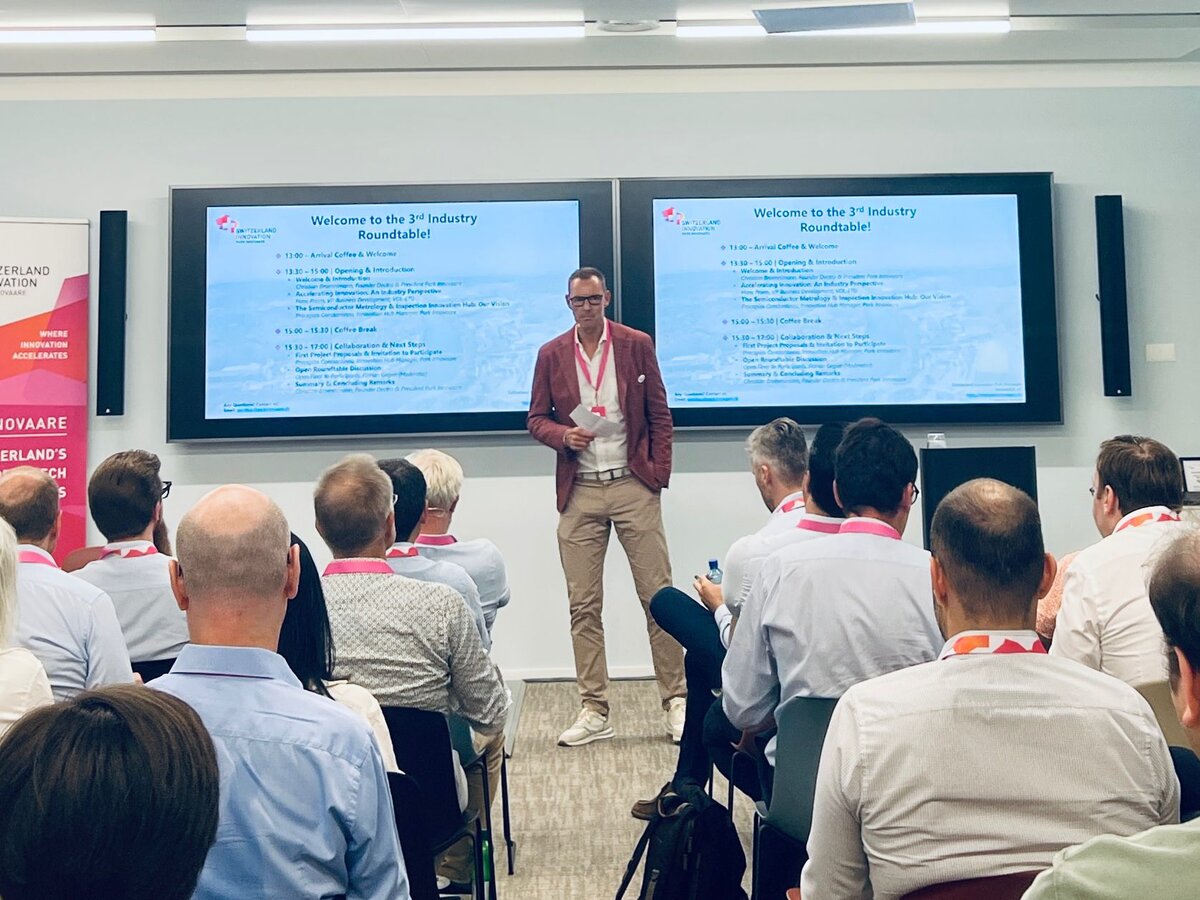
To accelerate collaboration and drive impact, the SeMI Innovation Hub introduces two complementary event formats—bringing together industry leaders and members to exchange insights, define priorities, and co-create future initiatives.
Industry Roundtable
The Industry Roundtable is a half‑day, interactive, afternoon event for professionals across the semiconductor metrology and inspection sector. Hosted by the SeMI Innovation Hub, this session features moderated discussions, peer‑to‑peer exchanges, and networking opportunities designed to explore current challenges, identify key industry pain points and highlight emerging R&D frontiers.
Our goal is to bring together a diverse community of stakeholders from across the sector to share insights and provide feedback on how the SeMI Hub can support progress, foster collaboration and address common challenges through shared resources and strategic research partnerships.
Date: 24 June 2026
Location: Park Innovaare
Registration: Detailed program and registration information will be available soon.
Semiconductor Metrology Workshop
The Semiconductor Metrology Workshop is a full-day, conference-style event bringing together professionals and academics from across the semiconductor metrology and inspection sector. Hosted by the SeMI Innovation Hub, the workshop will feature keynote presentations, industry insights, academic research and closing panel discussions.
Our goal is to connect representatives from public institutions, research organizations, and private companies, highlighting the latest achievements in the field from other leading national and international hubs. This workshop aims to serve as a vibrant platform for showcasing innovation, fostering knowledge exchange and strengthening collaborative networks within Switzerland’s semiconductor ecosystem.
Date: 27 October 2026
Location: Park Innovaare
Registration: Detailed program and registration information will be available soon.
Strategic Goals
A proactive hub enabling innovation and technology development by bridging PSI's top science with industry’s market needs through collaborative R&D in semiconductor metrology & inspection.
1. | Drive Innovation Activity with Swiss Industry |
2. | Accelerate Research Activity at PSI |
3. | Catalyze Ecosystem Activity |
| Deliver value to industry through collaborative R&D with the Hub serving as the on-site interface that initiates, guides and manages industry-defined projects with PSI, giving simple access to its world‑class research facilities and expertise. | |
| PSI as an anchor to drive more global, high-value research collaborations, with the Hub proactively driving outreach and accelerating industry-relevant research activities. | |
| A forward-looking ecosystem that drives business and research activity, strengthens Switzerland’s innovation capacity and position in the semiconductor sector, whilst translating PSI's scientific output and advances into a strategic knowledge pool. |
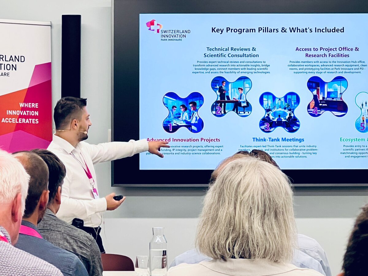
5 Key Pillars
Navigating a major research institution like PSI can be complex and time‑consuming - we make that journey simpler. The SeMI Innovation Hub provides a streamlined interface that enables industry partners to initiate collaborative R&D projects and access local facilities. Our framework is built on 5 strategic pillars that guide projects from initial brainstorming to final execution.
1. Think-Tank Meetings
We bring industry experts together in one place to identify current challenges, brainstorm creative solutions, and incubate innovative ideas specifically within the field of semiconductor metrology and inspection.
2. Technical Reviews & Scientific Consultation
We translate complex research into practical insights. We bridge knowledge gaps, assess emerging technology trends, and conduct pilot studies to ensure that every idea has a solid scientific and technical foundation.
3. Lighthouse Projects
We manage collaborative R&D projects born from our earlier stages. This pillar focuses on guiding feasibility, implementation, IP/NDA management, and securing funding to deliver high-impact outcomes for the industry.
4. Access to Project Office & Research Facilities
We provide the physical space and tools needed for success. Partners gain access to shared office spaces and streamlined entry to lab and research infrastructure, supporting the seamless execution of R&D projects at every stage.
5. Ecosystem & Network Access
The foundation of our success is a select group of industry partners and experts. This network is engaged across all pillars, driving action and collaboration while continuously growing and strengthening the global innovation community.
Roadmap 2030
The hub is designed for the long term. The year 2026 marks the official launch phase, during which the first members will be recruited and start-up funding from the Canton of Aargau secured. By 2030, the SeMI Hub is set to achieve operational self-sufficiency through membership fees and specialised analytical services. Through this collaboration, Park Innovaare creates a decisive locational advantage and positions itself as a central hub for global semiconductor innovation.
2026 | Launch and Growth of Membership |
2027 - 2029 | Start Flagship Projects |
2026 - 2030 | Establish Lighthouse Projects |
2030 | Operational Self-Sustainability |
Join us as a SeMI Hub Partner!
More than 20 companies are actively supporting the initiative and have signed a ‘Letter of Support’. In doing so, they commit to being part of the network, recognising the Innovation Hub as a strategic partner, and actively driving the development of market-ready solutions. The partners cover the entire value chain – from global market leaders to specialist suppliers.
As a non‑profit initiative, the SeMI Innovation Hub provides a platform that delivers strategic value and tangible benefits to its partners while fostering a collaborative community committed to achieving meaningful results together. All partnership fees directly support the establishment and ongoing activities of the Innovation Hub, enabling us to maintain a vibrant and engaging innovation ecosystem for all partners.
Partner Benefits
Lead & Participate in collaborative “Lighthouse” R&D projects with PSI using a structured, safe, NDA‑protected collaboration framework.
Use the Hub as you're on‑site interface with PSI to initiate, co‑execute, and manage projects that enhance your R&D outcomes with less operational overheads than doing it yourself.
Simple access to PSI’s world‑class facilities and scientific expertise.
- Connection to a strategic knowledge pool, leveraging the Hubs birds-eye view of the research and industry ecosystem.
Partnership Fees
Small Companies
This program is designed for smaller companies with <50 full-time equivalents.
CHF 3'000/year *
Large Companies
This option is intended for companies with >50 full-time equivalents.
CHF 10'000/year *
* 25% Discount for shareholders & Park Innovaare companies
Get in contact with us today
Dr. Procopios Constantinou, Project Manager, SeMI Innovation Hub will be happy to advise and connect you.
Office: +41 79 688 70 75
E-Mail